Products

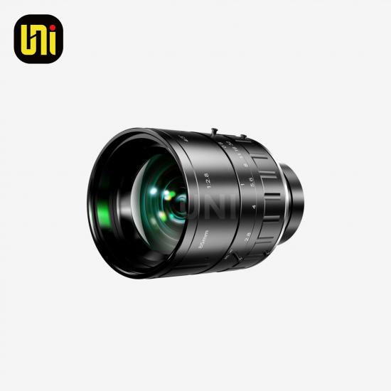
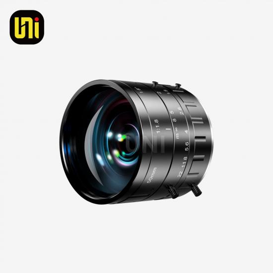
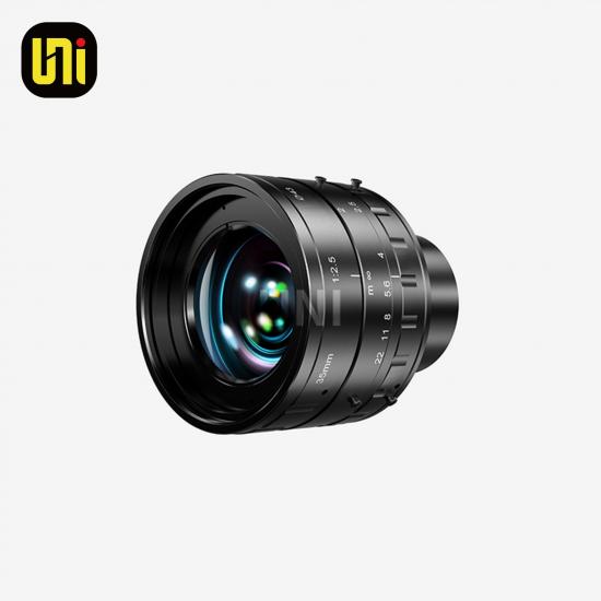
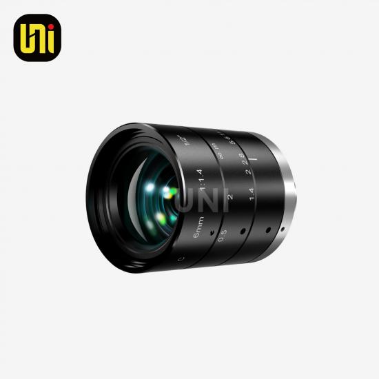
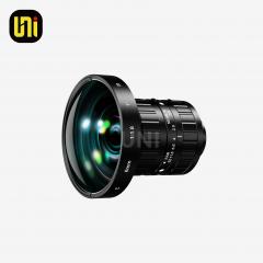
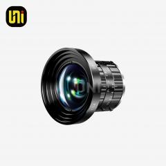
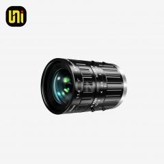
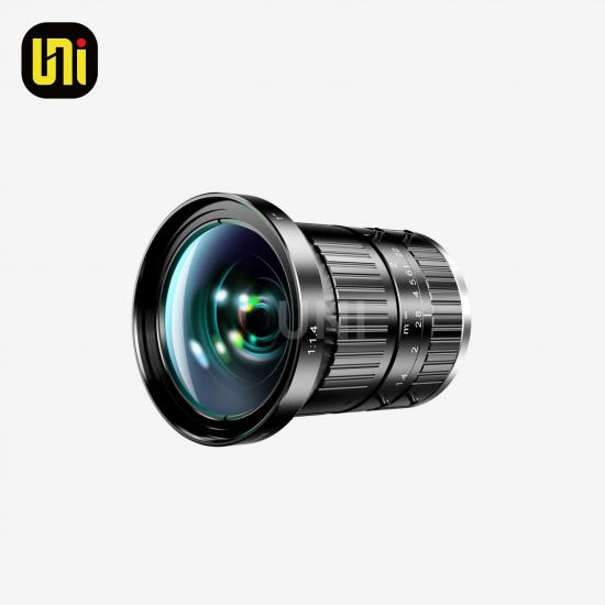
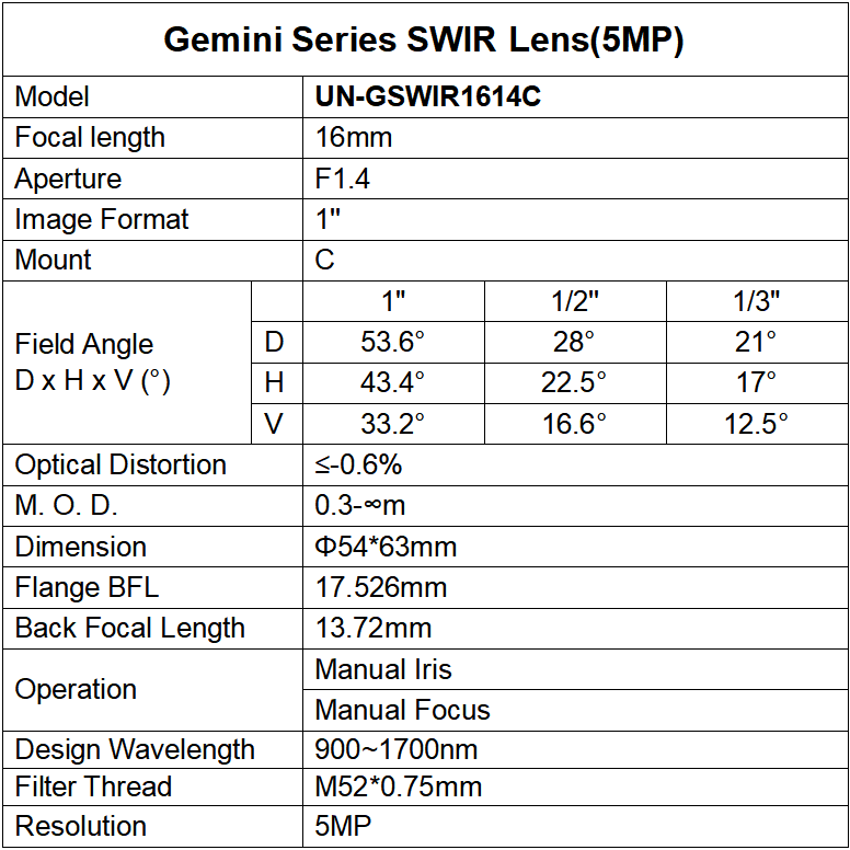
SWIR Lens UN-GSWIR1614C

For Automated Optical Inspection (AOI), Food Sorting, Recycling Sorting, etc.


· Developed for 1" image format
· Wavelength: 900-1700nm
· Large Aperture, upto F1.4
· Compact and lightweight design
Inquiry now
  • description

Send a Message
If you have any problem when using the website or our products, please write down your comments or suggestions, we will answer your questions as soon as possible!Thank you for your attention!
If you have questions or suggestions,please leave us a message,we will reply you as soon as we can!
Related Products
SWIR Lens UN-GSWIR0618C

For Security Surveillance, Vehicle & Drone Obstacle Avoidance, Semiconductor Wafer Inspection, etc.


· Developed for 1" image format

· Wavelength: 900-1700m

· Large Aperture, up to F1.4

· Compact and lightweight design
SWIR Lens UN-GSWIR1214C

For Vision-Guided Positioning Systems, Semiconductor Defect Inspection, Agricultural Remote Sensing Imaging, Hyperspectral Camera, etc.


· Developed for 1" image format
· Wavelength: 900-1700nm
· Large Aperture, up to F1.4
· Compact and lightweight design
SWIR Lens UN-GSWIR10020C

For Semiconductor Wafer Inspection, Wildfire Detection & Ember Monitoring, etc.


· Developed for 1" image format
· Wavelength: 900-1700nm
· Large Aperture, up to F1.4
· Compact and lightweight design
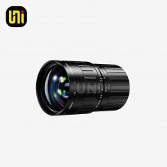
SWIR Lens UN-GSWIR752S-14MP

For Semiconductor Wafer Inspection, Biomedical Imaging, Logistics Package Sorting, Wildfire Detection & Ember Monitoring, etc.


· Developed for 1.1" image format
· Wavelength: 800-1700nm
· Large Aperture, up to F2.0
· Compact and lightweight design

SWIR Lens UN-GSWIR0814CL

For Hyperspectral Camera, Fruit & Vegetable Sorting Equipment, Perovskite Solar Cell Defect Detection


· Developed for 1" image format
· Wavelength: 900-1700nm
· Large Aperture, up to F1.4
· Compact and lightweight design
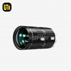


SWIR Lens UN-GSWIR2514C

For Photovoltaic Inspection, Pill / Capsule Detection, Print Inspection, Hyperspectral Camera, etc.


· Developed for 1" image format
· Wavelength: 900-1700nm
· Large Aperture, up to F1.4
· Compact and lightweight design
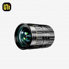
SWIR Lens UN-GSWIR3514C

For Security Recognition & Hyperspectral Camera, Semiconductor Wafer Inspection, Biomedical Imaging, Logistics Package Sorting, Wildfire Detection & Ember Monitoring, etc.


· Developed for 1" image format
· Wavelength: 900-1700nm
· Large Aperture, up to F1.4
· Compact and lightweight design
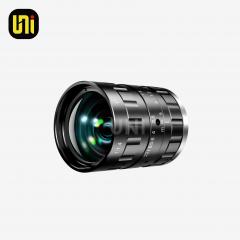
SWIR Lens UN-GSWIR5014C

For Semiconductor Wafer Inspection, Biomedical Imaging, Logistics Package Sorting, Wildfire Detection & Ember Monitoring, etc.


· Developed for 1" image format
· Wavelength: 900-1700nm
· Large Aperture, up to F1.4
· Compact and lightweight design
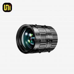
V-Mount Line Scan LensUN-CLS954.5/V45

For lithium battery electrode, copper foil and ceramic separator inspection, PCB & single-layer FPC AOI detection, silicon wafer routine sorting, food packaging & label printing quality control and electronic ceramic substrate inspection.


· Covering a wide working distance range

· Very low distortion and high resolution

· Lockable distance and aperture settings


Product information: Custom designs are available upon request.
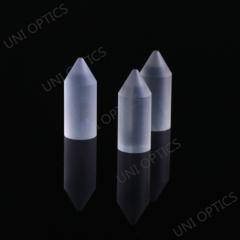

Micro Size Lens
Micro Size Lens
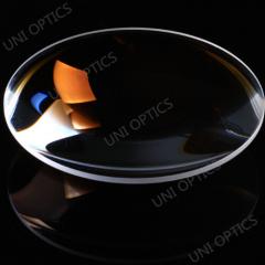
Micro Size Lenses are commonly used in miniature imaging, sensing, and illumination applications where compact size is essential. Their small dimensions enable efficient light collection and focusing in tight spaces. UNI Optics offers a range of Micro Size Lenses in various materials for performance from the ultraviolet to the NIR.
IR Optics material
Infrared Optics Material

1Silicon (Si) 


Silicon (Si) is grown by Czochralski pulling techniques (CZ) and contains some oxygen that causes an absorption band at 9 microns.To avoid this, material can be prepared by a Float-Zone (FZ) process. Optical silicon is generally lightly doped (5 to 40 ohm cm) for best transmission above 10 microns, and doping is usually boron (P-type) and phosphorus (N-type). After doping silicon has a further pass band: 30 to 100 microns which is effective only in very high resistivity uncompensated material.
 
CZ Silicon is commonly used as substrate material for infrared reflectors and windows in the 1.5-8 micron region. The strong absorption band at 9 microns makes it unsuitable for CO2 laser transmission applications, but it is frequently used for laser mirrors because of its high thermal conductivity and low density. Application as window, lens in the 1.5 - 8 um region; Mirror for CO2 laser and spectrometer applications.
 

Crystallographic properties
Syngony Cubic
Lattice Constant, A 5.43
Physical properties
Density 2.33g/cm3
Hardness, Mohs 7
Dielectric Constant for 9.37 x 10⁹ Hz 13
Melting point, оС 1414
Thermal Conductivity, W/m·K at 313 K 163
Thermal Expansion, 1/K at 293 K 2.6x10⁻⁶
Specific Heat Capacity, J/(kg°C) 712.8
Bandgap, eV 1.1
Knoop Hardness, kg/mm2 1100
Youngs Modulus, Gpa 130.91
Shear Modulus, GPan 79.92
Bulk Modulus, GPa 101.97
Debye Temperature, K 640
Poissons Ratio 0.28
Chemical properties
Solubility in water None
Molecular Weight 28.09

2. ZnS material:


ZnS MultiSpectral Under intense heat and pressure, defects within the crystalline lattice are virtually eliminated, leaving a water-clear material with minimal scatter and high transmission characteristics from 0.4 to 12 microns. This material is particularly well suited for high-performance common aperture systems that must perform across a broad wavelength spectrum.

Specifications:

Material: ZnS MultiSpectral
Diameter Tolerance: --------------------- +0.0, -0.1mm
Thickness Tolerance: -------------------- ±0.1mm
Clear Aperture: ---------------------------->85%
Parallelism: -----------------------------------3 arc minute
Surface Quality: ----------------------------80-50 scratch and dig
Wavefront Distortion: -------------------- λ /2 per 25mm @633mm
Bevel: -----------------------------------------Protective  (<0.2mm x 45° )
Coating: -------------------------------------- Optional (Uncoated, AR Coating, etc.)


3. ZnSe material


ZnSe is a preferred material for lenses, windows, output couplers and beam expanders for its low absorptivity at infrared wavelengths and its visible transmission. For high-power applications, it’s critical that the material bulk absorption and internal defect structure be carefully controlled, that minimum-damage polishing technology be employed, and the highest quality optical thin-film coatings are used. The material absorption is verified by CO2 laser vacuum calorimetry. Our quality assurance department provides testing and specific optics certification on request.

ZnSe is non-hygroscopic and chemically stable, unless treated with strong acids. It’s safe to use in most industrial field, and laboratory environments.


Line Scan Lens UN-ALS1164L-16K

For high-end PCB AOI inspection, Mini/Micro LED panel micro-defect detection, photovoltaic silicon wafer EL hidden crack inspection, narrow precision metal strip flaw detection, luxury printing anti-counterfeit texture inspection, electronic ceramic substrate microscopic inspection and high-precision linear dimension measurement of tiny electronic components.


· Developed for 66mm big frame sensor
· Low distortion
· Compatible for 16K line scan camera
· Excellent optical performance, uniform imaging of center and edge

Product information: Custom designs are available upon request.

Subscribe Our Newsletter
get in touch
  • Facebook
  • Youtube
  • Linkedin
  • ins
REQUEST A FREE QUOTE
If you have any problem when using the website or our products, please write down your comments or suggestions, we will answer your questions as soon as possible!Thank you for your attention!

Copyright © UNI OPTICS CO., LTD © All Rights Reserved.

leave a message

Home

Products

COMPANY

Contact